AND/OR Package
(by DL5UY)
The B5x00 hardware is solely made of discrete components like resistors, capacitors, diodes and transistors. No tubes are used. All transistors and diodes are germanium type.
In some places inductors, transformers and delay lines are used.
Potentiometers are used for adjustment of voltages or timing.
The central main oscillator uses crystal and a tank inductor.
The logic itself is basically diode transistor logic or DTL:
https://en.wikipedia.org/wiki/Diode%E2%80%93transistor_logic
Note that in this Wikipedia article NPN transistors are shown and the collector supply voltage is positive in regard to ground.
However, when the B5x00 Design was made in the late 1950s/early 1960s, the common and fastest Transistors were Germanium PNP transistors. Hence the collector supply voltage is negative in regard to ground level. In all circuit diagrams this fact may be confusing at first, since diode and transistor symbol arrows point in the technical current flow direction from plus to minus and not in the more “logical” electron flow direction from minus to plus.
For that reason, FALSE logic level is about 0 V, TRUE logic level is a negative voltage of about -4.8 V!
The B5x00 logic uses four different supply voltages:
Notes:
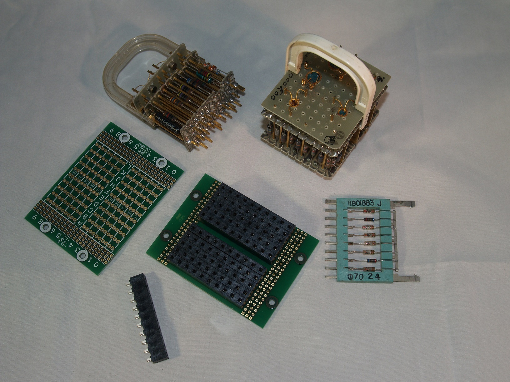
The core logic of a B5x00 is split into three distinct package types:
This concept works perfect if you alternate active packages with AND/OR packages. Note:
AND/OR Package
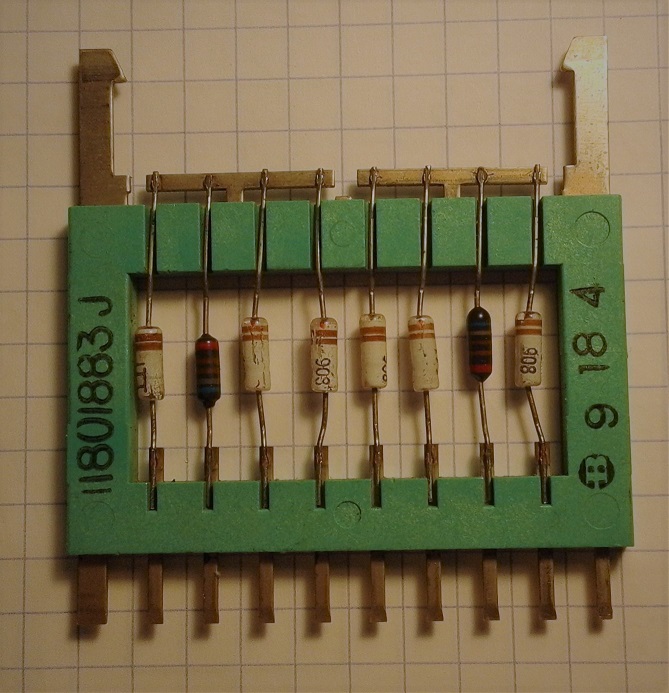
The AND/OR package has 10 pins and is equipped with six germanium diodes and two 6.81k resistors. All are connected together with the metallic bar at the top of the package. The diodes' cathodes are connected to the bar. This bar can be intentionally cut to divide the package into having two smaller AND/OR gates.
For the ease of discussion, we designate those pins as COM1, D1, R1, D2, D3, D4, D5, R2, D6, COM2.
When the bar is not cut we can realise a 5-input AND/OR gate, by connecting the input signals to 5 diodes and one of the two resistors to -12 V. The other resistor must be left unconnected.
One of the diodes is the output, which can be wire-ORed with other such outputs.
The number of AND inputs can be expanded in increments of six by just using several AND/OR packages connected at their COM1/COM2 pins. In total only one resistor should be connected to -12 V.
When the bar is cut like in the package shown above, the result is two 2-input AND/OR gates consisting of three diodes each and one resistor.
The OR package has 10 pins and is equipped with eight germanium diodes. All are connected together with the metallic bar at the top of the package. The anodes are connected to the bar.
When an OR package is used after an AND/OR package, all diodes of the AND/OR package can be used for inputs (effectively making it an AND only package) and the COM1 or COM2 pins go to inputs of the OR package.
Examples: AND/OR Package Schematics
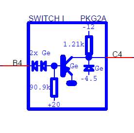
SWITCH I package
The SWITCH I package contains five independently useable inverters:
Since the emitter is grounded, the TRUE logic level input voltage is raised by the two diodes at the left. Those are are actually silicon diodes with roughly 0.6 V of drop each. That brings the TRUE logic level to about -1.5 V.
As stated before, in almost every active package, the inputs lead directly or through some diodes to the base of a transistor. The signal source must provide a current limitation. The TRUE level signal is clamped to about -1.5 V. The TRUE level output is clamped to about -4.8 V by a germanium diode to -4.5 V.
Here you can see a demonstration of the signal levels of a SWITCH I:
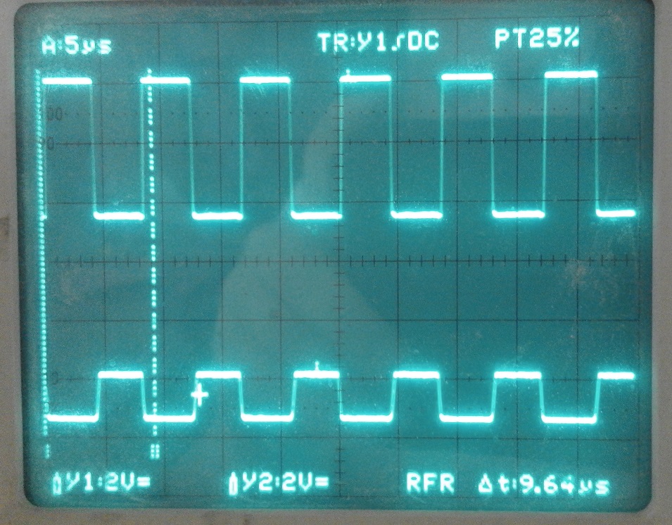
Oscilloscope of Signals
Here is the haywire test circuit used to get the signal levels:
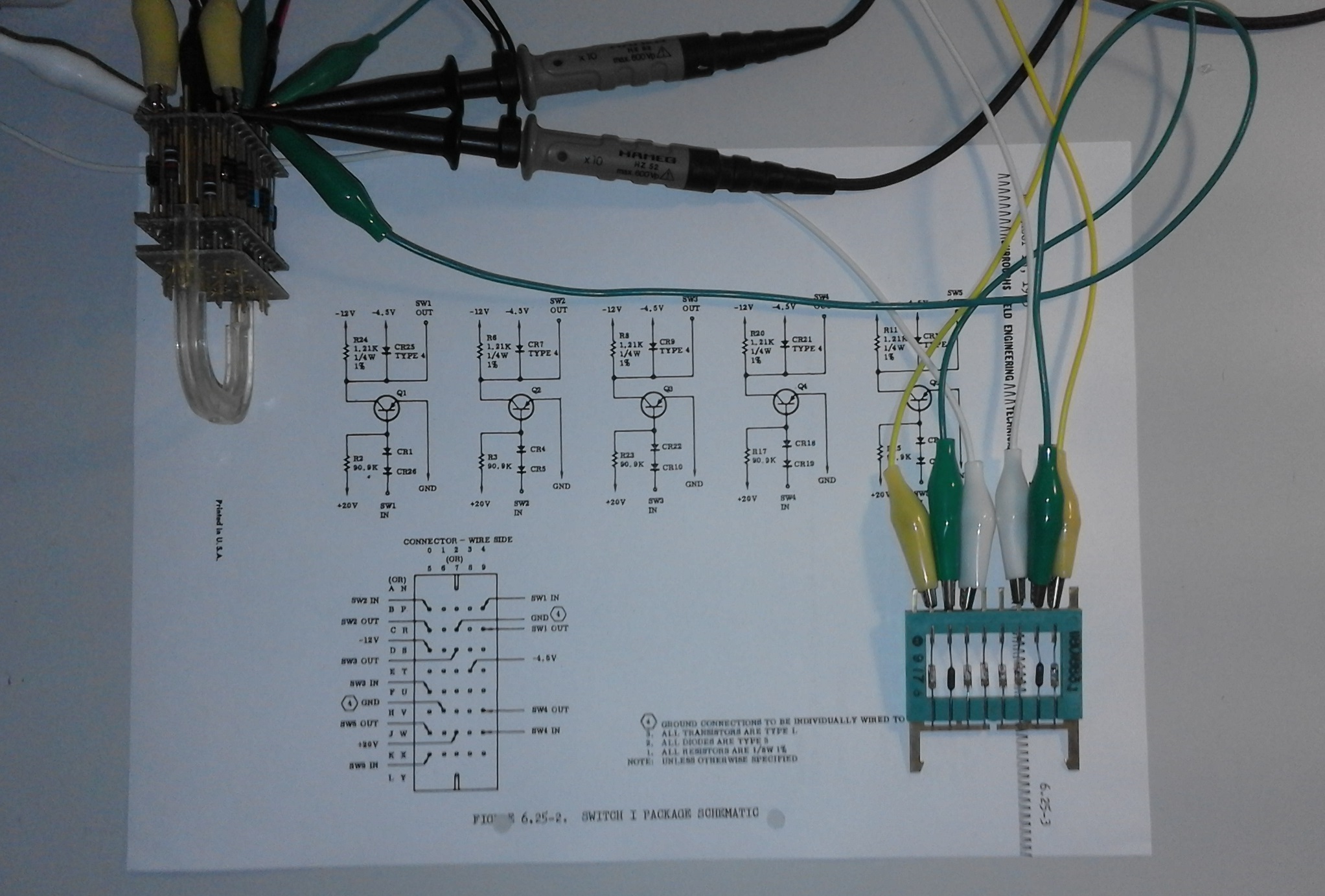
Test Circuit
Here is the circuit diagram of that setup: SWITCH I Test Circuit Schematics
I made a small printed circuit board which will allow a more reliable wiring and even a working demonstration using several modules and diode sticks. The connectors are not the original ones, but do work well. Only at the “A” end some dremeling was be needed to accommodate the wider pins. The way those connectors are made makes this an easy task.
Test adapters